


- Windows
- Prisms
- Spherical Lenses
- Cylindrical Lenses
- Mirrors
- Beamsplitters
- Polarization Optics
- Singlet True Zero Order Waveplate
- Cemented True Zero Order Waveplate
- Cemented Zero Order Waveplate
- Optical Contact Zero Order Waveplate
- Air-Spaced Zero Order Waveplate
- Low Order Waveplate
- Multi-Order Waveplate
- Narrow Band Polarization Beamsplitter Cube
- Broadband Polarization Beamsplitter Cube
- Rotator
- Glan Taylor Polarizer
- Glan Laser Polarizer
- Glan Thompson Polarizer
- Glan Thompson Polarization Beamsplitter Cube
- Wollaston Polarizer
- Rochon Polarizer
- Broadband Polarization Beam Combiner
- Brewster Polarizer
- Brewster Window
- Coatings


Singapore team launches silicon photonics follow-up
Second phase of packaging program follows successful development of device library including grating couplers.
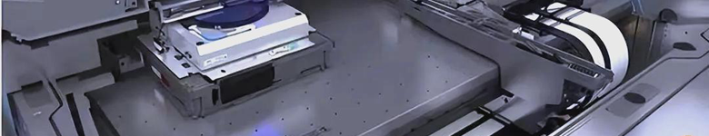
Silicon photonics device development
The A*STAR Institute of Microelectronics (IME) in Singapore has launched a new industry consortium that will look to build on the success of its silicon photonics development with new packaging expertise.
Driven by an anticipated need for faster, smaller and cheaper optical links to support the emerging Internet of Things, IME will work with industry partners including Corning, Fujikura, Accelink Technologies, and NTT in the second phase of its silicon photonics effort.
Laser diode integration
Together with experts at the Heinrich Hertz Institute in Germany, they will work to develop a broad range of packaging techniques, as well as low-loss coupling modules, and solutions for laser diode integration.
New thermal models and management are also on the agenda, along with better reliability and RF performance, with A*STAR saying: “All these new developments will lead to a more integrated packaging solution which promises better assembly margins and lower module costs.”
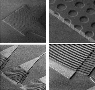
During the first phase of the silicon photonics work, the team developed so-called “tool boxes” and a device library to enable the integration of low-profile lateral fiber assembly with laser diodes and other photonics devices.
“By employing a laser welding technique, the consortium demonstrated a fiber-chip-fiber loss of less than 8 dB with less than 1.5 dB excess packaging loss,” claims the lab.
More specifically, they produced a silicon grating coupler with a 2D grating designed to “achieve polarization diversity performance”, as well as reducing the coupling loss on a 220 nm-thick silicon-on-insulator base.
Kenji Nishide from Fujikura’s Advanced Technology Laboratory commented: “Silicon photonics packaging is a crucial technology for the commercialization of silicon photonic devices. The partnership generated remarkable results [during Phase I], and we are pleased to continue with the second phase, which will expand the application of silicon photonics with innovative approaches in terms of laser diode integration and RF performance.
“Through this consortium, Fujikura will accelerate the development of compact and cost-effective optical communications for diverse markets.”
MEMS team
IME has also set up an industry consortium to develop MEMS packaging technology. According to the A*STAR team, the problem with conventional chip stacking that relies on a through-silicon via (TSV) and wire bonding on substrate method is that it usually results in high costs and large form factors.
A consortium including Delta Electronics, InvenSense and ULVAC will now aim to reduce production costs and shrink device sizes by developing a TSV-free, over-mold, wafer-level packaging solution for MEMS-capped wafers.
It will rely on a novel metal-deposited silicon pillar and wire bonding for through-mold interconnects.
California-based InvenSense’s VP of technology and worldwide manufacturing Mo Maghsoudnia said in a statement issued by A*STAR: “Currently, it is anticipated that the demand for sensors will grow from billions to trillions by 2050.
“This demand is being driven by the emergence of sensor-based smart systems fusing computing, connectivity and sensing in the context of the Internet of Things. IME’s packaging consortia partnership will allow us to identify and develop MEMS packaging innovative solutions in order to scale up for the Internet of Things”